
AT89C51 is an 8-bit microcontroller and belongs to Atmel’s 8051 family. ATMEL 89C51 has 4KB of Flash programmable and erasable read only memory (PEROM) and 128 bytes of RAM. It can be erased and program to a maximum of 1000 times.
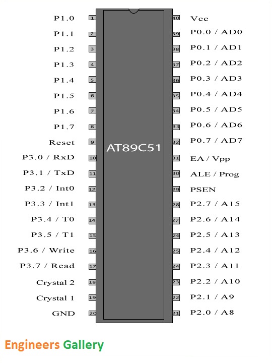
In 40 pin AT89C51, there are four ports designated as P1, P2, P3 and P0. All these ports are 8-bit bi-directional ports, i.e., they can be used as both input and output ports. Except P0 which needs external pull-ups, rest of the ports have internal pull-ups. When 1s are written to these port pins, they are pulled high by the internal pull-ups and can be used as inputs. These ports are also bit addressable and so their bits can also be accessed individually.
Port P0 and P2 are also used to provide low byte and high byte addresses, respectively, when connected to an external memory. Port 3 has multiplexed pins for special functions like serial communication, hardware interrupts, timer inputs and read/write operation from external memory. AT89C51 has an inbuilt UART for serial communication. It can be programmed to operate at different baud rates. Including two timers & hardware interrupts, it has a total of six interrupts.
Pin Description:
| Pin No | Function | Name | ||
| 1 | 8 bit input/output port (P1) pins | P1.0 | ||
| 2 | P1.1 | |||
| 3 | P1.2 | |||
| 4 | P1.3 | |||
| 5 | P1.4 | |||
| 6 | P1.5 | |||
| 7 | P1.6 | |||
| 8 | P1.7 | |||
| 9 | Reset pin; Active high | Reset | ||
| 10 | Input (receiver) for serial communication | RxD | 8 bit input/output port (P3) pins | P3.0 |
| 11 | Output (transmitter) for serial communication | TxD | P3.1 | |
| 12 | External interrupt 1 | Int0 | P3.2 | |
| 13 | External interrupt 2 | Int1 | P3.3 | |
| 14 | Timer1 external input | T0 | P3.4 | |
| 15 | Timer2 external input | T1 | P3.5 | |
| 16 | Write to external data memory | Write | P3.6 | |
| 17 | Read from external data memory | Read | P3.7 | |
| 18 | Quartz crystal oscillator (up to 24 MHz) | Crystal 2 | ||
| 19 | Crystal 1 | |||
| 20 | Ground (0V) | Ground | ||
| 21 | 8 bit input/output port (P2) pins/High-order address bits when interfacing with external memory | P2.0/ A8 | ||
| 22 | P2.1/ A9 | |||
| 23 | P2.2/ A10 | |||
| 24 | P2.3/ A11 | |||
| 25 | P2.4/ A12 | |||
| 26 | P2.5/ A13 | |||
| 27 | P2.6/ A14 | |||
| 28 | P2.7/ A15 | |||
| 29 | Program store enable; Read from external program memory | PSEN | ||
| 30 | Address Latch Enable | ALE | ||
| Program pulse input during Flash programming | Prog | |||
| 31 | External Access Enable; Vcc for internal program executions | EA | ||
| Programming enable voltage; 12V (during Flash programming) | Vpp | |||
| 32 | 8 bit input/output port (P0) pinsLow-order address bits when interfacing with external memory | P0.7/ AD7 | ||
| 33 | P0.6/ AD6 | |||
| 34 | P0.5/ AD5 | |||
| 35 | P0.4/ AD4 | |||
| 36 | P0.3/ AD3 | |||
| 37 | P0.2/ AD2 | |||
| 38 | P0.1/ AD1 | |||
| 39 | P0.0/ AD0 | |||
| 40 | Supply voltage; 5V (up to 6.6V) | Vcc | ||
- 172287 reads