RTC DS 12C887 is widely used to provide exact time and date in many applications such as x86 IBM PC. This RTC provides time components hour, minute and second in addition to the date/calendar components of year, month and day. This chip uses an internal lithium battery, which keeps the time and date updated even when the power is off. The DS12C887 works on CMOS technology to keep the power consumption low. It has a total of 128 bytes of non volatile RAM. It uses 14 bytes of RAM for storing the values of clock/calendar and control registers. The rest 114 bytes of RAM are for general purpose data storage.
The internal registers are accessible only when the RTC is powered by an external power source. When the external power is turned off, the RTC clock keeps running from the internal lithium battery source but the internal registers of the RTC cannot be accessed. RTC 12C887 becomes active when a voltage greater than 4.25V is applied and the internal registers can be accessed after 200 msec.
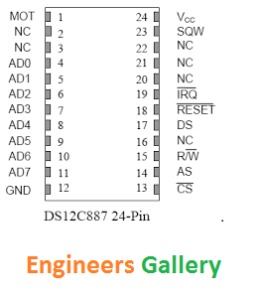
Click here for the pin diagram of DS12C887.
The RTC DS12C887 is a 24 pin IC. Its pin description is as follows:
| Pin no. | Pin name | Pin description |
| 1 | MOT | The MOT pin is used to select between the Motorola and Intel bus types. When connected to VCC, Motorola bus timing is selected. When connected to GND or left disconnected, Intel bus timing is selected. |
| 2-3 | NC | Not connected pins |
| 4-11 | AD0-AD7 | These pins act as a bidirectional address and data lines of the RTC. The addresses are present during the first portion of the bus cycle and the same pins are used for data in the second portion of the cycle. |
| 12 | GND | Chip ground. |
| 13 | CS | Chip select is an active low input pin. CS must be low in order to access the chip during read (RD) and write (WR) operation while using with Intel controllers and vice versa for Motorola controllers. |
| 14 | AS | This pin is used to demultiplex the address and data. A positive going pulse on this pin serves to demultiplex the bus. The falling edge of the pulse causes the address to be latched within the DS12C887. |
| 15 | R/W | This pin is used to read/write data from the RTC. It operates in two modes depending on bus timing selected using the MOT pin.When Intel timing (MOT= GND) is selected, the R/W pin functions as a write enable pin which is active low.The explanation of the Motorola bus timing (MOT=VCC) is out of the scope of this article. |
| 16 | NC | Not connected pin |
| 17 | DS | The DS/RD (data strobe/read input) pin has also has two modes of operation depending on the bus timing selected using MOT pin. When the Intel bus timing is selected (MOT=GND), DS pin functions as an active low read pin.The explanation of the Motorola bus timing (MOT=VCC) is out of the scope of this article. |
| 18 | RESET | This is an active low pin and resets all the interrupts and flags. It does not affect the clock, calendar or RAM. It should be kept high to access the RTC. |
| 19 | IRQ | This is an active low interrupt pin of the RTC and remains high by default. It is used as interrupt input for the controller. This pin remains low until the status bit status pin causing the interrupt is present and the corresponding interrupt-enable bit is set. The IRQ pin gets clear either by the reset pin or by reading the C register. |
| 20-22 | NC | Not connected pins |
| 23 | SQW | The SQW pin is an output pin used to generate square waves of predefined frequencies. The frequency of the SQW pin can be selected by programming register A. The SQW signal can be turned on and off using the SQWE bit in Register B. |
| 24 | Vcc | +5V. |
RTC DS12C887 has three interrupts, namely, Alarm interrupt, Periodic interrupt & Update interrupt. For detailed information, refer RTC interrupts.
Address Map of the DS12C887:
The DS12C887 has a total of 128 bytes of RAM space with address 00-7FH. The first ten locations, 00-09, are set aside for RTC values of time, calendar, and alarm data. The next four locations 10-13 (0A-0D in hex) are reserved for the control and status registers A, B, C, and D. The next 114 bytes from address 0EH-7FH are available for general purpose data storage.
All the registers are accessible directly except:
Registers C and D are read only.
D7 bit of register A is read only.
The following table shows the address map of the RTC.
| Address Location | Purpose |
| 0x00 | Seconds |
| 0x01 | Seconds Alarm |
| 0x02 | Minutes |
| 0x03 | Minute Alarm |
| 0x04 | Hours |
| 0x05 | Hours Alarm |
| 0x06 | Day of the week |
| 0x07 | Day of the Month |
| 0x08 | Month |
| 0x09 | Year |
| 0x0A | Register A |
| 0x0B | Register B |
| 0x0C | Register C |
| 0x0D | Register D |
| 0x0E-0x7F | General Purpose |
Address location for time, calender and alarm:
The values of the time, calendar and date can be assessed by reading the corresponding byte from the memory of RTC. The RTC 12C887 can provide and accept data for the values of time, date and calendar in two formats i.e., Binary and BCD. The format of the data can be selected by using the DM pin of the Register B. If DM is set to 1, it signifies binary mode and a 0 in DM signifies BCD mode.
Before writing any data the SET bit in register B should be made high. This will prevent any updates to occur. When the data writing is over the SET bit should be cleared i.e., should be made low to restart the updates. The data format for time, date and calendar should be same.
The table below shows the values of time, date and calendar in the two data formats.
| Address | Function | Decimal Value | DATA MODE RANGE | |
| Binary(hex) | BCD | |||
| 0 | SECONDS | 0-59 | 00-3B | 00-59 |
| 1 | SECONDS ALARM | 0-59 | 00-3B | 00-59 |
| 2 | MINUTES | 0-59 | 00-3B | 00-59 |
| 3 | MINUTES ALARM | 0-59 | 00-3B | 00-59 |
| 4 | HOURS, 12-HOUR MODEHOURS, 12-HOUR MODEHOURS, 24-HOUR MODE | 1-121-120-23 | 01-0C AM81-8C PM0-17 | 01-12 AM81-92 PM0-23 |
| 5 | HOURS ALARM, 12-HOURHOURS ALARM, 12-HOURHOURS ALARM, 24-HOUR | 1-121-120-23 | 01-0C AM81-8C PM0-17 | 01-12 AM81-92 PM0-23 |
| 6 | DAY OF THE WEEK, SUN=1 | 1-7 | 01-07 | 01-07 |
| 7 | DAY OF THE MONTH | 1-31 | 01-1F | 01-31 |
| 8 | MONTH | 1-12 | 01-0C | 01-12 |
| 9 | YEAR | 0-99 | 00-63 | 00-99 |
Control Registers of RTC DS12C887
The RTC DS 12C887 has four control register for its various operations. The explanation of each of the control register is as follows.
REGISTER A
The details of the register A are shown in the table below:
| BIT 7 | BIT 6 | BIT 5 | BIT 4 | BIT 3 | BIT 2 | BIT 1 | BIT 0 |
| UIP | DV2 | DV1 | DV0 | RS3 | RS2 | RS1 | RS0 |
| Register Bits | Purpose |
| UIP | Update In Progress. It is a read only bit used to monitor the update status of the RTC. The 1 on UIP indicates that the update is about to occur. A 0 on the UIP indicates that no updates will happen for at least 244us and any information of time calendar and alarm can be accessed from the RTC. It is not affected by reset pin. The updates can be stopped by setting the SET bit of register B to 1. |
| DV2, DV1, DV0 | These pins are used to turn on or off the oscillator. The pattern 010 will turn on the oscillator and the RTC will start keeping the time. The next update will occur at 500ms after the pattern 010 is written |
| RS3,RS2, RS1,RS0 | These pins are used to set the frequency of the square wave which is generated at pin number 23 of the RTC. |
REGISTER B
| BIT 7 | BIT 6 | BIT 5 | BIT 4 | BIT 3 | BIT 2 | BIT 1 | BIT 0 |
| SET | PIE | AIE | UIE | SQWE | DM | 24/12 | DSE |
| Register bits | Purpose |
| SET | When the SET bit is 0, the update transfer functions works normally and the clock is updated once per second. When the SET bit is a 1, the updates are stopped. |
| PIE | Periodic interrupt enable pin. When this pin is set to 1, periodic interrupts are generated on the IRQ pin. The rate of generating the interrupt is decided by the RS3-RS0 bits of Register A. |
| UIE | Update ended interrupt enable pin. This is a read/write pin used to enable the update end interrupt. Every time an update occurs, the update end flag (UF) in register C gets set and the IRQ pin goes low. |
| SQWE | Square wave enable. When this pin is set to a 1, a square wave is produced at the SQW pin. The frequency of the square wave is specified by the settings at pins RS3-RS0 |
| DM | Data mode. This pin is used to set the mode of data. A 1 signifies binary data while a 0 signifies BCD data format. |
| 24/12 | This bit is used to select between 12/24 hour mode. A 1 indicates 24 hour mode and a 0 indicates 12 hour mode. |
| DSE | Daylight saving enable bit. This pin is used to enable the two special updates when set to 1. |
REGISTER C
The register C is read only register. The first four least significant bits are not used and therefore set to 0. This register tells the status of the interrupts.
| BIT 7 | BIT 6 | BIT 5 | BIT 4 | BIT 3 | BIT 2 | BIT 1 | BIT 0 |
| IRQF | PF | AF | UF | 0 | 0 | 0 | 0 |
| Register bits | Purpose |
| IRQf | Interrupt request flag. This bit is set to 1 whenever at least one of the interrupt occurs. |
| PF | Periodic interrupt flag. This bit is set to 1 when the periodic interrupt occurs. |
| AF | Alarm interrupt flag. This bit is set to one when the alarm interrupt occurs i.e., current time matches the alarm time. |
| UF | Update Ended interrupt flag. This bit is set to 1 after every update cycle has occurred. |
| Bit 3-0 | Unused bit. These bit always read zero. |
REGISTER D
| BIT 7 | BIT 6 | BIT 5 | BIT 4 | BIT 3 | BIT 2 | BIT 1 | BIT 0 |
| VRT | 0 | 0 | 0 | 0 | 0 | 0 | 0 |
- VRT: Valid RAM and Time. This is a read only pin used to indicate the condition of the internal lithium battery. A 0 on this pin indicates a bad state of lithium battery and the data of the RTC is questionable and should not be used. A 1 indicates healthy state of the internal battery with reliable data.
- BIT 6 through BIT 0 – The remaining bits of Register D are not usable. They cannot be written and, when read, they will always read 0.





Post Comment
You must be logged in to post a comment.