Analog to digital converters find huge application as an intermediate device to convert the signals from analog to digital form. These digital signals are used for further processing by the digital processors. Various sensors like temperature, pressure, force etc. convert the physical characteristics into electrical signals that are analog in nature.
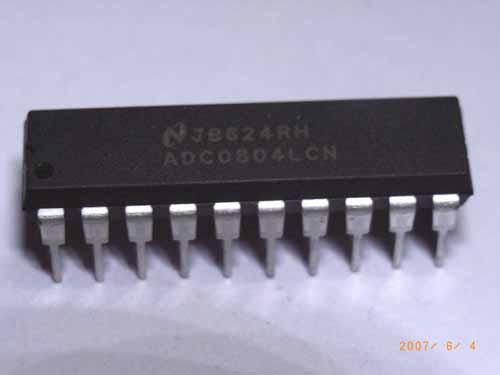
ADC0804 is a very commonly used 8-bit analog to digital convertor. It is a single channel IC, i.e., it can take only one analog signal as input. The digital outputs vary from 0 to a maximum of 255. The step size can be adjusted by setting the reference voltage at pin9. When this pin is not connected, the default reference voltage is the operating voltage, i.e., Vcc. The step size at 5V is 19.53mV (5V/255), i.e., for every 19.53mV rise in the analog input, the output varies by 1 unit. To set a particular voltage level as the reference value, this pin is connected to half the voltage. For example, to set a reference of 4V (Vref), pin9 is connected to 2V (Vref/2), thereby reducing the step size to 15.62mV (4V/255).
ADC0804 needs a clock to operate. The time taken to convert the analog value to digital value is dependent on this clock source. An external clock can be given at the Clock IN pin. ADC 0804 also has an inbuilt clock which can be used in absence of external clock. A suitable RC circuit is connected between the Clock IN and Clock R pins to use the internal clock.
DataSheet:
Analog to digital converters find huge application as an intermediate device to convert the signals from analog to digital form. These digital signals are used for further processing by the digital processors. Various sensors like temperature, pressure, force etc. convert the physical characteristics into electrical signals that are analog in nature.
ADC0804 is a very commonly used 8-bit analog to digital convertor. It is a single channel IC, i.e., it can take only one analog signal as input. The digital outputs vary from 0 to a maximum of 255. The step size can be adjusted by setting the reference voltage at pin9. When this pin is not connected, the default reference voltage is the operating voltage, i.e., Vcc. The step size at 5V is 19.53mV (5V/255), i.e., for every 19.53mV rise in the analog input, the output varies by 1 unit. To set a particular voltage level as the reference value, this pin is connected to half the voltage. For example, to set a reference of 4V (Vref), pin9 is connected to 2V (Vref/2), thereby reducing the step size to 15.62mV (4V/255).
ADC0804 needs a clock to operate. The time taken to convert the analog value to digital value is dependent on this clock source. An external clock can be given at the Clock IN pin. ADC 0804 also has an inbuilt clock which can be used in absence of external clock. A suitable RC circuit is connected between the Clock IN and Clock R pins to use the internal clock.
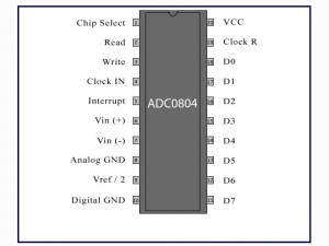
Pin Diagram:
Pin Description:
| Pin No | Function | Name |
| 1 | Activates ADC; Active low | Chip select |
| 2 | Input pin; High to low pulse brings the data from internal registers to the output pins after conversion | Read |
| 3 | Input pin; Low to high pulse is given to start the conversion | Write |
| 4 | Clock Input pin; to give external clock. | Clock IN |
| 5 | Output pin; Goes low when conversion is complete | Interrupt |
| 6 | Analog non-inverting input | Vin(+) |
| 7 | Analog inverting Input; normally ground | Vin(-) |
| 8 | Ground(0V) | Analog Ground |
| 9 | Input pin; sets the reference voltage for analog input | Vref/2 |
| 10 | Ground(0V) | Digital Ground |
| 11 | 8 bit digital output pins | D7 |
| 12 | D6 | |
| 13 | D5 | |
| 14 | D4 | |
| 15 | D3 | |
| 16 | D2 | |
| 17 | D1 | |
| 18 | D0 | |
| 19 | Used with Clock IN pin when internal clock source is used | Clock R |
| 20 | Supply voltage; 5V | Vcc |



Post Comment
You must be logged in to post a comment.