I2C(Inter Integrated Circuit)/TWI(Two Wire Interface)
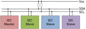
The I2C bus physically consists of 2 active wires and a ground connection. The active wires, called SDA and SCL, are both bi-directional. SDA is the Serial DAta line, and SCL is the Serial Clock line.
The I2C bus is a multi-master bus. This means that more than one IC capable of initiating a data transfer can be connected to it. The I2C protocol specification states that the IC that initiates a data transfer on the bus is considered the Bus Master. Consequently, at that time, all the other ICs are regarded to be Bus Slaves. It is depending on clock pulse so that it called as Synchronous communication.
I2C/TWI is a half-duplex serial transmission and hence the data flow can be in a direction at a time. The data transfer rate depends on crystal frequency of slave controller. The rate of data transfer refers to clock frequency on SCL bus which must be 1/16th of slave frequency.
Capable Length of protocol is depends on the load of the bus and the speed you run at. In typical applications, the length is a few meters (9-12ft). Another thing to be taken into account is the amount of noise picked up by long cabling. The length can be increased significantly by running at a lower clock frequency. One particular application – clocked at about 500Hz – had a bus length of about 100m (300ft). If you are careful in routing your PCB’s and use proper cabling (twisted pair and/or shielded cable), you can also gain some length.
Features:
8 bit data bite oriented transfer.
It is capable to handle maximum 128 devices(depend on clock frequency)
Speed is 100Kbps in standard mode and 400Kbps in Fast mode, also 5Mbps in high speed mode.
Only two bus are required for communication for each device
Specific address for each Slave
Each device can be as Master/Slave
Also worked as Multi Master/ Multi slave serial communication
As mentioned above I2C has two mail lines SDA for data and SCL for Clock pulse also need pullup resister to both buss for Bus Idle condition.
There needs to be a third wire which is just the ground or 0 volts. There may also be a 5volt wire is power is being distributed to the devices. Both SCL and SDA lines are “open drain” drivers. What this means is that the chip can drive its output low, but it cannot drive it high. For the line to be able to go high you must provide pull-up resistors to the 5v supply. There should be a resistor from the SCL line to the 5v line and another from the SDA line to the 5v line. You only need one set of pull-up resistors for the whole I2C bus, ot for each device
Protocol sequence:
Send the START bit (S).
Send the slave address (ADDR) include point 3.
Send the Read(R)-1 / Write(W)-0 bit.
Wait for/Send an acknowledge bit (A).
Send/Receive the data byte (8 bits) (DATA).
Expect/Send acknowledge bit (A).
Send the STOP bit (P).
The Real Communication:
As we saw already, the active lines used for communication in I²C protocol are bi-directional. Each & every device (for example: MCU, LCD driver, ASIC, remote I/O ports, RAM, EEPROM, data converters) connected to the bus will be having a unique address. Each of these devices can act as a receiver and/or transmitter, depending on the functionality. And also each device connected to the bus is software addressable by this unique address.
As we already know the nodes or any other peripheral devices (no matter whether its master or slave) use micro controllers to connect and communicate through the bus, this communication can be considered as inter-IC communication in general.
Let us assume that the master MCU (as always, it’s the master who initiates the communication) wants to send data to one of its slaves. The step-by-step procedure will be as follows.
Wait until it sees no activity on the I2C bus. The SDA and SCL lines are both high. The bus is ‘free’.
The Master MCU issues a start condition, telling that “its mine – I have started to use the bus”. Thiscondition informs all the slave devices to listen on the serial data line for instructions/data.
Provide on the SCL line a clock signal. It will be used by all the ICs as the reference time at whicheach bit of data on the SDA line will be correct (valid) and can be used. The data on the data line must be valid at the time the clock line switches from ‘low’ to ‘high’ voltage.The Master MCU sends the unique binary address of the target device it wants to access.
Master MCU puts a one-bit message (called read/write flag) on the bus telling whether it wants toSEND or RECEIVE data from the other chip. This read/write flag is an indication to the slave nodewhether the access is a read or a write operation.
The slave node ICs will then compare the received address with its own address. The Slave devicewith the matching address responds back with an acknowledgement signal. If the address doesn’tmatch, they simply wait until the bus is released by the stop condition.
Once the master MCU receives the acknowledgment signal, it starts transmitting or receiving andthe data communication proceeds between the Master and the Slave on the data bus. Both themaster and slave can receive or transmit data depending on whether the communication is a read orwrite. The transmitter sends 8-bits of data to the receiver, which replies with a 1-bit acknowledgment. And the action of data transfer continues.
When the communication is complete, the master issues a stop condition indicating that everythingis done. This action free ups the bus. The stop signal is just one bit of information transferred by aspecial ‘wiggling’ of the SDA/SCL wires of the bus.
Protocol Detail:
Every byte put on the SDA line must be eight bits long. The number of bytes that can be transmitted per transfer is unrestricted. Each byte must be followed by an Acknowledge bit. Data is transferred with the Most Significant Bit (MSB) first to LSB last.
For each clock pulse one bit of data is transferred. The SDA signal can only change when the SCL signal is low – when the clock is high the data should be stable.


Post Comment
You must be logged in to post a comment.