You might have seen that how to make a PCB, but before making PCB you must have knowledge about how to make layout for making PCB!
There are so many softwares by which we can make layouts such as KiCad, OrCAD, eagle, spice etc. Here we will discuss about KiCad and we are going to use it for making layout.
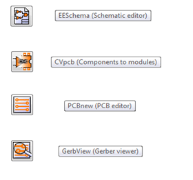
Here is the small introduction about KiCad, its much user friendly and its little bit easy to understand too. In KiCad we have to follow total 4 steps to complete layout of pcb. These steps are as shown in picture.
For brief details of KiCad, just google it!
1. EESchema (schematic editor)–
In this step we have to draw the schematic for required circuit.
2. CVpcb (components to modules)-
This step shows how to assign footprints to a particular component.
3. PCBnew (PCB editor)-
Here actually you have to draw the tracks according to your wiring made in EESchema.
The width of track can be adjusted according to our requirement.
4. GerbView (Gerber Viewer)-
To send your board to a manufacturer you will need to generate a gerber file.
See for the Downloads to start at the end. [sam id=”5″ codes=”true”]







Post Comment
You must be logged in to post a comment.