Programmable central control unit manufactured by many companies in the market, there are many microcontroller in a similar price range and variety of features. The STM32F429 was chosen for this project.STMicroelectronics STM32F429 produced by the company is a software development kit.
2 temperature sensor in the project in general, there are 8 digital outputs and 4 timers. Data from temperature sensors that measure one of them will transmit wirelessly to the main board. Wireless to it, which is independent from the main system requires a separate system. It needs its own microcontroller in accordance with its own temperature sensor and RF module is a module design made to measure wireless temperature. NRF24L01 developed by Nordic companies are used for data transmission with RF communication.
LM35 temperature sensor is used as the temperature sensor developed by Texas Instruments company. Its unique design with atmega328p-pin microcontroller as part of the RF module is selected.
LCD Display and Menu Design
In line with the project design needs to be done in menus using available information about the LCD is concerned. Project, as previously mentioned eight separate digital output control, sensor 2, and 4 includes a separate timer. The display and control make this information available is almost impossible one. To be checked or to be shown because of the extra data is needed is a menu design. The first page of the menu, the main menu consists of 3 separate pages that can be accessed from the main menu. This 3 separate pages respectively Sensors, Timers sekmeleridir.me STM32 design the LEDs and GUI Builder is used. This tab prior written writing on the main menu view, then the main screen menu view type was created rectangular space filled with the background to give and to bring this view becomes more elegant was put into a black rectangle frames the perimeter of the rectangular area. These frames are placed at specific coordinates.Hereinafter, this starting and ending frames where x, y values by utilizing when the screen is pressed, this area will have the opportunity to program the following menu Skip to shape our system. We have a single display plane and could consider as one page. Menu design is also required us pages. This need has been assigned to a variable page in order to meet all the screen during the transition and are cleaned every page.
ADC AND TEMPERATURE SENSOR LM35
There are 2 LM35 temperature sensor in the project. One is connected directly to stm32’y, thanks to the data is read from the sensor contains the ADC process. ADC channel ADC conversion process for the Project 13, the ADC 3 is used. ADC has been working as an independent mode.In front raters it has the Div 2 setting. So the operating speed of the bus is connected AHB1 works at half speed. This means 90MHz. ADC takes place by way of example. This sampling time is defined as the 3-hour cycle of the project and has been assigned as a 5-hour waiting period between two sampling cycles.
The STM32 ADC resolution is 12 bits. That results measured value sensor and the 5V ADC we feed process, we need to multiply 5000.#FFFH To turn that result in ° C to 4096 (2 12), we need to value the division. This value, as well as the sensor section is 10mV / ° C linear scale, we must compartment. This processing is obtained as a result of readings from sensors ° C.
GPIO SETUP AND DIGITAL OUTPUT
GPIO settings include settings to use general-purpose inputs and outputs assigned. 8 digital outputs to control located primarily in the project must be made of these settings. STM32 in the port from K up to 164 different GPIO pin setting is possible to do. This set 5 comprises separate portions.
- Gpıo_p of: Pins to be used is selected. 7 to 14 to be able to control 8 digital output pins are selected in the project.
- In gpıo_mo: pin mode is part of the set is determined as input or output. This setting has been selected as output for digital output control we do the project. There is also the AF mode. This mode is for setting the pins to be used in alternate functions such as SPI or USART communication.
- Gpıo_otyp to: push pull or open circuit vacant options are available.This value is set to push-pull digital output control.
- Gpıo_pupd: With this setting up or pull down resistor that can be defined for this setting can be omitted altogether or p. This is used in the project.
- gpıo_speed: it is the part that determines the operating speed of the P. 100MHz, 50MHz, 25MHz and 2MHz 4 separate value as specified. Because there is no requirement about this section of the project it has been selected as arbitrary 100MHz.
Port settings made with the pin code is defined gpıo_ınit after these settings. GPIO is selected in the project. Thus, PE7, PE8, PE9, PE10, PE11, PE12, PE13 and PE14 as digital output pins are available for use.
Before the program is designed for digital output control menu after setting the GPIO LEDs are controlled options in this section. 8 of 8 green LEDs in the red There are 16 separate square. They open the digital output of the green ones, red ones are designated as digital outputs switch on. Determining the switch / case when the cycle of opening and closing codes printed in this area is active and the LED is on.
RF MODULE AND NRF24L01
The project is located 2 temperature sensor. Bunlardan1 of them will transfer data wirelessly. Wireless independently working on part of the main card is required to transfer data to an RF module design. This RF module will be designed which will make both temperature measurement, the value measured will send stm32’y as well as wireless. The RF module is required to have a microcontroller to perform these operations. 28pinl of preferred atmega328p-pin microcontrollers from Atmel has been selected.
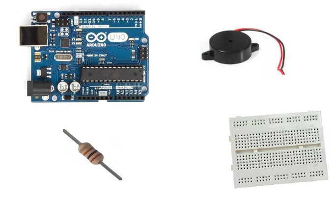
Atmel programming kit is required for atmega328p-pin programming.This microcontroller is a microcontroller Arduino UNO is also owned.Atmel microcontroller programming kit instead of using this facility can be programmed in line with the Arduino UNO. Atmega328p-pin microcontroller, we need to install the boot loader to use in this way.
RF module schematic is as follows.
Measurement of temperature with LM35 is like we have done in the STM32. Here atmega328p-pin processor instead of 10-bit resolution while reading the C cycle because the process ADC with 2 ^ 10 4096 1024, so we must compartment. Other operations are the same.
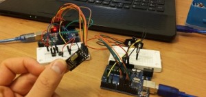
After we did the microcontroller and temperature measurements of the wireless module stm32’y we need to transfer it wirelessly. Here are put NRF24L01 module in Figure 6.3. NRF24L01 The Nordic companies are working on low-power 2.4GHz RF module which was developed by the.Operating voltage 1.9 V 3.6 V stand. Communication distance is approximately 250 meters in open space. This module works as both receiver and transmitter. There are six separate bus module. So the possibility of sending data 1 There are 5 separate modules one module.All modules of 5 bytes in length has its own private addresses. The modules will be installed when the communication between the receiver or transmitter module and the identification of the address must be determined. The maximum length of the data sent to the module is 32byt. Tx and Rx module address can be determined by the user or default settings may be used. Module 125 has a separate channel. This channel selectivity were determined in the 2.4 GHz 2.525ghz 125 takes place in separate channels. The data transfer speed 2Mbps, 1Mbps and 250kbps can be selected. The output module is 0dBm, -6dB, -12dB or -18dbm can be selected. The module is also available to IQRQ p, also has a cutting function.
The module communicates with the microcontroller through the SPI communications. The module itself has a special method to send data.This method relies on the address given, Tx load recorder, then the data to be written into that address is selected, then the length of the data which is to be sent is specified. These opcodes are shown in more detail.In the same way, and recorded in the registers of the submitted data Tx module, Rx module of the recorder, we need to read the same way.
RF receiver module in part, that similar operations have been implemented in the STM32 side. Spi1 pin package for those who SPI communication module is used first. So MOSI, MISO and SCK pins, respectively PA7, PA6 and PA5 pins are used. PG9 and PG10 and CSN pins GPIO pins for CE settings are made. 50MHz output speed is assigned to the CE and CSN pins.
Timers
Timers are programmed to a specific time runs out. That is, a digital output is set off time fixed off time. There are 4 timer in the project.Real-time employees must be an hour before we have to give an outlet to the timer feature. STM32 from internal RTC (Real Time Clock) is located. This function is defined and controlled through RTC library. The RTC also has a recorder in the nature STM32 savior. If the interruption of power STM32 board does not return to the hour when restarted, it will continue to run from where it left hours thanks to this recorder. With real-time system clock is set to the RTC library. There are 4 timer in the project. These designated days, hours and minutes are scheduled to begin work on the specified end date and time to work again.



Post Comment
You must be logged in to post a comment.