It is responsibility of design engineer to get the most performance and capability out of the resources available in limited budget and that too for specific application requirements.
While the ideas presented here are around Atmel’s 89S52 microcontroller, these can be easily used with all other types of microcontrollers without any changes and configurations. This note discusses two such techniques to save microcontroller IO lines.
Interfacing 3×2 Keys

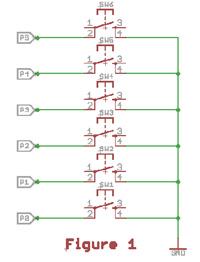
Usually in order interface 3×2 keys i.e. 6 keys, we will need six IO pins of microcontroller to take inputs. The basic schematic is shown in figure 1.
However, in regular practice we usually recommend using matrix scanning method to interface more keys where keys are arranged in row-column format and then can be scanned one by one. In such case, we will need 3 rows and 2 columns (or vice versa) to interface 3×2 keys as shown in figure 2. That means 5 IO pins are still required for interfacing.
Here is the third novel technique to reduce required IO pins further. This technique needs some additional (yet cheaper) hardware though. As shown in

schematic Figure 3, keys are connected in set of three keys each.
Each set has small signal switching diode connected in series (typical component recommended is 1N4148). Note the direction of diodes in each set as it is reversed in one set as against another.
In order to identify which key has been pressed; specific algorithm needs to be deployed as explained here. First pin P0 should be set to logic HIGH while P1 and P2 to logic LOW. Then after fractional delay, read input status at P1 and P2. If P1 is found HIGH, this means the path, P0-B2-D2-P1 is complete i.e. button B2 has been pressed. However, if P2 is found HIGH, that would mean P0-D5-B5-P2 is complete i.e. button B5 is pressed. Similarly, when P1 is set to HIGH keeping P0 and P2 LOW; B1 and B4 can be identified. Buttons B3 and B6 can be detected by setting P2 to HIGH and reading status of P0 and P1 respectively. Table 1 shows logical combinations for above mentioned algorithm to be used alongwith the circuit as per figure 3.

Here the only hardware addition is of six small signal diodes which would not be a cost burdon on the design yet help in saving 2 to 4 IO pins.




Post Comment
You must be logged in to post a comment.