Semiconductor Basics
Introduction
[nextpage title=”Introduction” ]
If Resistors are the most basic passive component in electrical or electronic circuits, then we have to consider the Signal Diode as being the most basic “Active” component. However, unlike a resistor, a diode does not behave linearly with respect to the applied voltage as it has an exponential I-V relationship and therefore can not be described simply by using Ohm’s law as we do for resistors.
Diodes are basic unidirectional Semiconductor Devices that will only allow current to flow through them in one direction only, acting more like a one way electrical valve, (Forward Biased Condition). But, before we have a look at how signal or power diodes work we first need to understand the semiconductors basic construction and concept.
Diodes are made from a single piece of Semiconductor material which has a positive “P-region” at one end and a negative “N-region” at the other, and which has a resistivity value somewhere between that of a conductor and an insulator. But what is a “Semiconductor” material?, firstly let’s look at what makes something either a Conductor or an Insulator.
[/nextpage]
Resistivity
[nextpage title=”Resistivity” ]
The electrical Resistance of an electrical or electronic component or device is generally defined as being the ratio of the voltage difference across it to the current flowing through it, basic Ohm´s Law principals. The problem with using resistance as a measurement is that it depends very much on the physical size of the material being measured as well as the material out of which it is made. For example, if we were to increase the length of the material (making it longer) its resistance would also increase proportionally.
Likewise, if we increased its diameter or size (making it fatter) its resistance value would decrease. So we want to be able to define the material in such a way as to indicate its ability to either conduct or oppose the flow of electrical current through it no matter what its size or shape happens to be.
The quantity that is used to indicate this specific resistance is called Resistivity and is given the Greek symbol of ρ, (Rho). Resistivity is measured in Ohm-metres, ( Ω-m ). Resistivity is the inverse to conductivity.
If the resistivity of various materials is compared, they can be classified into three main groups, Conductors, Insulators and Semi-conductors as shown below.
Resistivity Chart
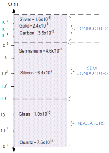 Notice that there is a very small margin between the resistivity of the conductors such as silver and gold, compared to a much larger margin for the resistivity of the insulators between glass and quartz.
Note also that the resistivity of all materials at any one time also depends upon their ambient temperature because metals are also good conductors of heat.
[/nextpage]
Conductors
[nextpage title=”Conductors” ]
From above we now know that Conductors are materials that have very low values of resistivity, usually in the micro-ohms per metre. This low value allows them to easily pass an electrical current due to there being plenty of free electrons floating about within their basic atom structure. When a positive voltage potential is applied to the material these “free electrons” leave their parent atom and travel together through the material forming an electron drift. In other words a current.
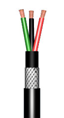
Examples of good conductors are generally metals such as Copper, Aluminium, Silver or non metals such as Carbon because these materials have very few electrons in their outer “Valence Shell” or ring, resulting in them being easily knocked out of the atom’s orbit. This allows them to flow freely through the material until they join up with other atoms, producing a “Domino Effect” through the material thereby creating an electrical current. Copper and Aluminium is the main conductor used in electrical cables as shown.
 An Electrical Cable uses
Conductors and Insulators
Generally speaking, most metals are good conductors of electricity, as they have very small resistance values, usually in the region of micro-ohms per metre. While metals such as copper and aluminium are very good conducts of electricity, they still have some resistance to the flow of electrons and consequently do not conduct perfectly.
The energy which is lost in the process of passing an electrical current, appears in the form of heat which is why conductors and especially resistors become hot. Also the resistivity of conductors increases with ambient temperature because metals are also generally good conductors of heat.
[/nextpage]
Insulators
[nextpage title=”Insulators” ]
Insulators on the other hand are the exact opposite of conductors. They are made of materials, generally non-metals, that have very few or no “free electrons” floating about within their basic atom structure because the electrons in the outer valence shell are strongly attracted by the positively charged inner nucleus.
So if a potential voltage is applied to the material no current will flow as there are no electrons to move and which gives these materials their insulating properties.
Insulators also have very high resistances, millions of ohms per metre, and are generally not affected by normal temperature changes (although at very high temperatures wood becomes charcoal and changes from an insulator to a conductor). Examples of good insulators are marble, fused quartz, p.v.c. plastics, rubber etc.
Insulators play a very important role within electrical and electronic circuits, because without them electrical circuits would short together and not work. For example, insulators made of glass or porcelain are used for insulating and supporting overhead transmission cables while epoxy-glass resin materials are used to make printed circuit boards, PCB’s etc. while PVC is used to insulate electrical cables as shown.
[/nextpage]
Semiconductor Basics
[nextpage title=”Semiconductor Basics” ]
Semiconductors materials such as silicon (Si), germanium (Ge) and gallium arsenide (GaAs), have electrical properties somewhere in the middle, between those of a “conductor” and an “insulator”. They are not good conductors nor good insulators (hence their name “semi”-conductors). They have very few “free electrons” because their atoms are closely grouped together in a crystalline pattern called a “crystal lattice”.
However, their ability to conduct electricity can be greatly improved by replacing or adding certain donor or acceptor atoms to this crystalline structure thereby, producing more free electrons than holes or vice versa. That is by adding a small percentage of another element to the base material, either silicon or germanium.
On their own Silicon and Germanium are classed as intrinsic semiconductors, that is they are chemically pure, containing nothing but semiconductive material. But by controlling the amount of impurities added to this intrinsic semiconductor material it is possible to control its conductivity. Various impurities called donors or acceptors can be added to this intrinsic material to produce free electrons or holes respectively.
This process of adding donor or acceptor atoms to semiconductor atoms (the order of 1 impurity atom per 10 million (or more) atoms of the semiconductor) is called Doping. The as the doped silicon is no longer pure, these donor and acceptor atoms are collectively referred to as “impurities”, and by doping these silicon material with a sufficient number of impurities, we can turn it into a semi-conductor.
The most commonly used semiconductor basics material by far is silicon. Silicon has four valence electrons in its outermost shell which it shares with its neighbouring silicon atoms to form full orbital’s of eight electrons. The structure of the bond between the two silicon atoms is such that each atom shares one electron with its neighbour making the bond very stable.
As there are very few free electrons available to move around the silicon crystal, crystals of pure silicon (or germanium) are therefore good insulators, or at the very least very high value resistors.
Silicon atoms are arranged in a definite symmetrical pattern making them a crystalline solid structure. A crystal of pure silica (silicon dioxide or glass) is generally said to be an intrinsic crystal (it has no impurities) and therefore has no free electrons.
But simply connecting a silicon crystal to a battery supply is not enough to extract an electric current from it. To do that we need to create a “positive” and a “negative” pole within the silicon allowing electrons and therefore electric current to flow out of the silicon. These poles are created by doping the silicon with certain impurities.
A Silicon Atom Structure
The diagram above shows the structure and lattice of a ‘normal’ pure crystal of Silicon.
N-type Semiconductor Basics
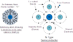
In order for our silicon crystal to conduct electricity, we need to introduce an impurity atom such as Arsenic, Antimony or Phosphorus into the crystalline structure making it extrinsic (impurities are added). These atoms have five outer electrons in their outermost orbital to share with neighbouring atoms and are commonly called “Pentavalent” impurities.
This allows four out of the five orbital electrons to bond with its neighbouring silicon atoms leaving one “free electron” to become mobile when an electrical voltage is applied (electron flow). As each impurity atom “donates” one electron, pentavalent atoms are generally known as “donors”.
Antimony (symbol Sb) or Phosphorus (symbol P), are frequently used as a pentavalent additive to the silicon as they have 51 electrons arranged in five shells around their nucleus with the outermost orbital having five electrons. The resulting semiconductor basics material has an excess of current-carrying electrons, each with a negative charge, and is therefore referred to as an N-type material with the electrons called “Majority Carriers” while the resulting holes are called “Minority Carriers”.
When stimulated by an external power source, the electrons freed from the silicon atoms by this stimulation are quickly replaced by the free electrons available from the doped Antimony atoms. But this action still leaves an extra electron (the freed electron) floating around the doped crystal making it negatively charged.
Then a semiconductor material is classed as N-type when its donor density is greater than its acceptor density, in other words, it has more electrons than holes thereby creating a negative pole as shown.
Antimony Atom and Doping
The diagram above shows the structure and lattice of the donor impurity atom Antimony.
P-Type Semiconductor Basics
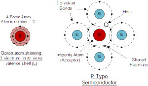
If we go the other way, and introduce a “Trivalent” (3-electron) impurity into the crystalline structure, such as Aluminium, Boron or Indium, which have only three valence electrons available in their outermost orbital, the fourth closed bond cannot be formed. Therefore, a complete connection is not possible, giving the semiconductor material an abundance of positively charged carriers known as holes in the structure of the crystal where electrons are effectively missing.
As there is now a hole in the silicon crystal, a neighbouring electron is attracted to it and will try to move into the hole to fill it. However, the electron filling the hole leaves another hole behind it as it moves. This in turn attracts another electron which in turn creates another hole behind it, and so forth giving the appearance that the holes are moving as a positive charge through the crystal structure (conventional current flow).
This movement of holes results in a shortage of electrons in the silicon turning the entire doped crystal into a positive pole. As each impurity atom generates a hole, trivalent impurities are generally known as “Acceptors” as they are continually “accepting” extra or free electrons.
Boron (symbol B) is commonly used as a trivalent additive as it has only five electrons arranged in three shells around its nucleus with the outermost orbital having only three electrons. The doping of Boron atoms causes conduction to consist mainly of positive charge carriers resulting in a P-type material with the positive holes being called “Majority Carriers” while the free electrons are called “Minority Carriers”.
Then a semiconductor basics material is classed as P-type when its acceptor density is greater than its donor density. Therefore, a P-type semiconductor has more holes than electrons.
Boron Atom and Doping
The diagram above shows the structure and lattice of the acceptor impurity atom Boron.
[/nextpage]
Semiconductor Basics Summary
[nextpage title=”Semiconductor Basics Summary” ]
N-type (e.g. doped with Antimony)
These are materials which have Pentavalent impurity atoms (Donors) added and conduct by “electron” movement and are therefore called, N-type Semiconductors.
In N-type semiconductors there are:
- 1. The Donors are positively charged.
- 2. There are a large number of free electrons.
- 3. A small number of holes in relation to the number of free electrons.
- 4. Doping gives:
- positively charged donors.
- negatively charged free electrons.
- 5. Supply of energy gives:
- negatively charged free electrons.
- positively charged holes.
P-type (e.g. doped with Boron)
These are materials which have Trivalent impurity atoms (Acceptors) added and conduct by “hole” movement and are therefore called, P-type Semiconductors.
In these types of materials are:
- 1. The Acceptors are negatively charged.
- 2. There are a large number of holes.
- 3. A small number of free electrons in relation to the number of holes.
- 4. Doping gives:
- negatively charged acceptors.
- positively charged holes.
- 5. Supply of energy gives:
- positively charged holes.
- negatively charged free electrons.
and both P and N-types as a whole, are electrically neutral on their own.
Antimony (Sb) and Boron (B) are two of the most commonly used doping agents as they are more feely available compared to other types of materials. They are also classed as “metalloids”. However, the periodic table groups together a number of other different chemical elements all with either three, or five electrons in their outermost orbital shell making them suitable as a doping material.
These other chemical elements can also be used as doping agents to a base material of either Silicon (S) or Germanium (Ge) to produce different types of basic semiconductor materials for use in electronic semiconductor components, microprocessor and solar cell applications. These additional semiconductor materials are given below.
Periodic Table of Semiconductors
| Elements Group 13 | Elements Group 14 | Elements Group 15 |
| 3-Electrons in Outer Shell (Positively Charged) |
4-Electrons in Outer Shell (Neutrally Charged) |
5-Electrons in Outer Shell (Negatively Charged) |
| (5)
Boron ( B )
|
(6)
Carbon ( C )
|
|
| (13)
Aluminium ( Al )
|
(14)
Silicon ( Si )
|
(15)
Phosphorus ( P )
|
| (31)
Gallium ( Ga )
|
(32)
Germanium ( Ge )
|
(33)
Arsenic ( As )
|
| (51)
Antimony ( Sb )
|
In the next tutorial about semiconductors and diodes, we will look at joining the two semiconductor basics materials, the P-type and the N-type materials to form a PN Junction which can be used to produce diodes.
[/nextpage]

